AMD ''Cato'' Review: the A9-9820 and RX-8120 Demystified
Published:
by:
Colonel Unicorn
Estimated reading time: ~31 minutes
So I Bought a Funny Motherboard…
Intro
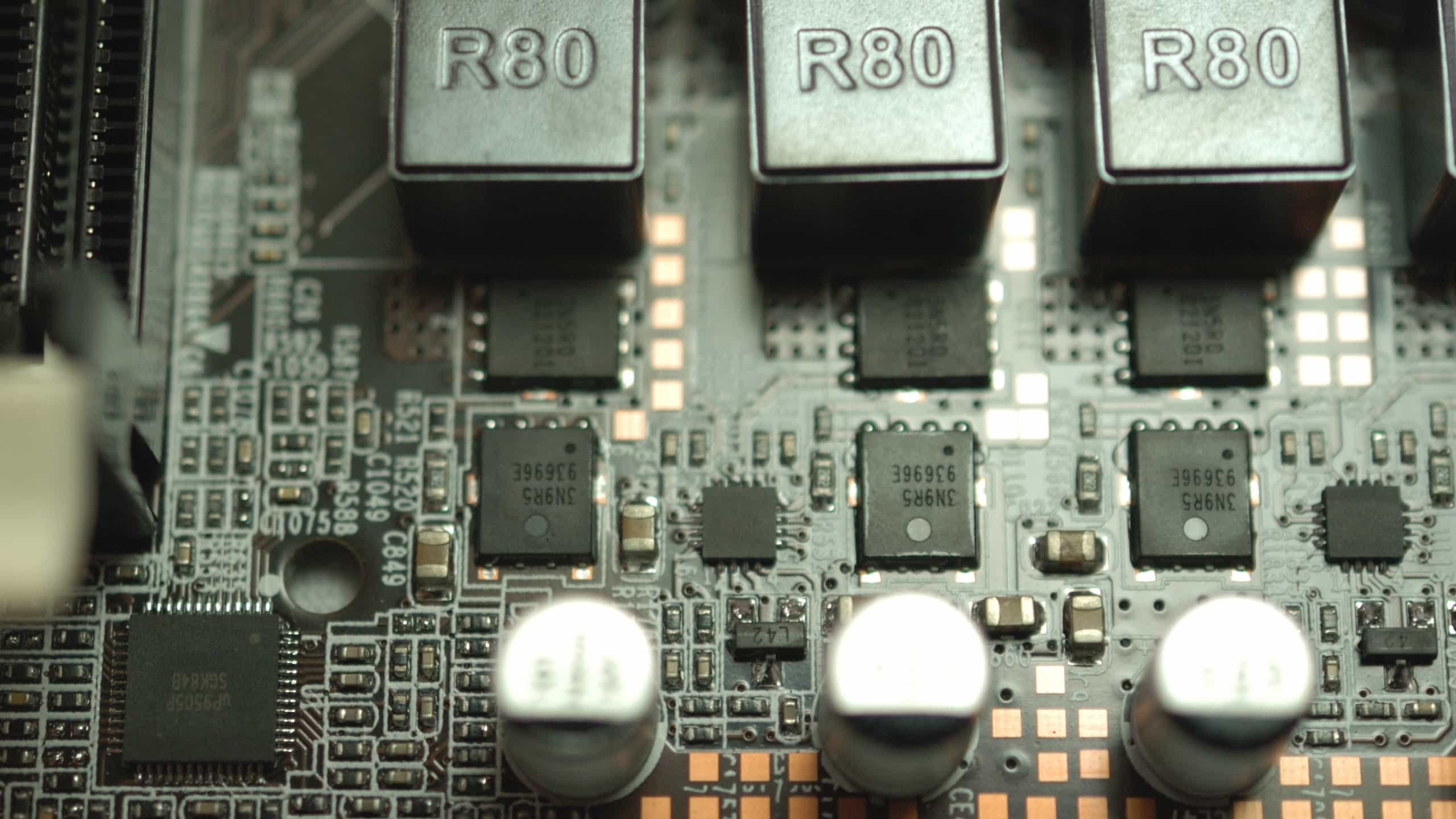
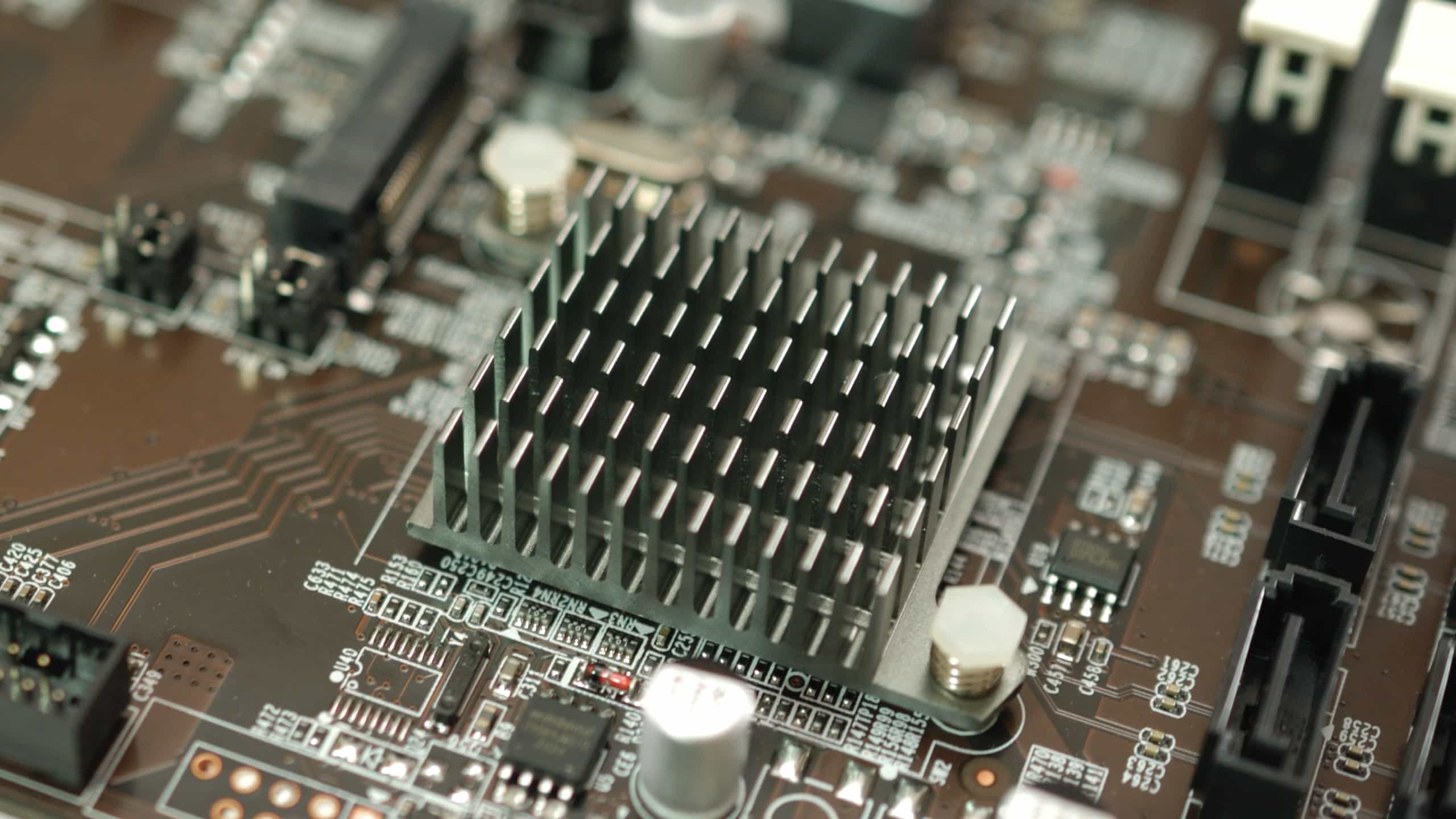
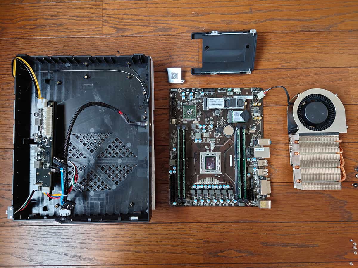
At first glance this appears to be a typical cheap microATX motherboard. Four DIMM slots arranged weird, a form-factor close to FlexATX but not quite, an expansion slot missing in one position and replaced with an M.2 slot in another, and a BGA processor that’s not a true SoC since it needs a separate chipset. The single video output and basic stereo audio suggest that this is meant to be used in a rather barebones system, perhaps an embedded system, but those tend to be green rather than this ugly brown. A set of dull, rectangular finstacks cool the chipset and VRMs. The only colorful part of the motherboard is the header for front-panel lights and buttons; every other slot, socket, and port is black. This is the sort of motherboard you’d find in a $300 Walmart special, not a shiny new gaming PC.
But I’m willing to overlook the spartan options and drab aesthetic for the novelty of a PC that uses an Xbox One APU.
I’ve wanted AMD to offer the Xbox One APU in a PC motherboard since 2013, and I never expected it to actually be made. It’s ironic that it’s only available now that the Xbox Series X is out. As soon as I learned it was available, I spent one-hundred and thirty-two United States dollars to ship a completely obsolete computer compoment with little hope of support from anybody in the supply chain from the other side of the planet, plus thirty-two dollarydoos for a kit of DDR3 because it isn’t even polite enough to boot with the RAM I had on hand.
But damn am I glad that this wasn’t available in 2013 because it would have cost a few hundred dollars mininum and, as a naive teenager and recent convert to PC, I actually would have had high hopes for it. My hopes today for anything approaching good performance have been thoroughly crushed. Waiting for benchmark runs to finish on an Athlon 5350 even with subambient cooling and a solid overclock will do that. This motherboard is only exciting now because it’s novel, but frankly it would’ve been mediocre in 2013 even if it had all the bells and whistles. It is completely obsolete now that Raven Ridge APUs exist. Actually I think my Crimson Canyon NUC would outperform this in nearly every metric, and the CPU in that thing is literally broken and was only ever sold because Intel needed to make shareholders happy.
Worst of all, even if you’re willing to accept that ok sure the seven-year-old APU based on a tablet architecture is kinda crap, you’re in for a rough time actually using it. The BIOS is half broken and AMD doesn’t officially distribute drivers, so you’re SOL if you want to use the GPU, which is kinda the point of a game console. Drivers are available, but the only public link is thanks to one guy in the Anglosphere who used a VPN to download them from a Japanese server that forbids foreign IP addresses and then hosted them on One Drive and dropped the link on the Linus Tech Tips forums.1 If you’re buying it new, then you can contact the seller, but I’m not sure how long they’ll be in business or how well they archive things.
Anyway, who wants to go down a rabbit hole?
So What Is This Exactly?
A Very Brief History
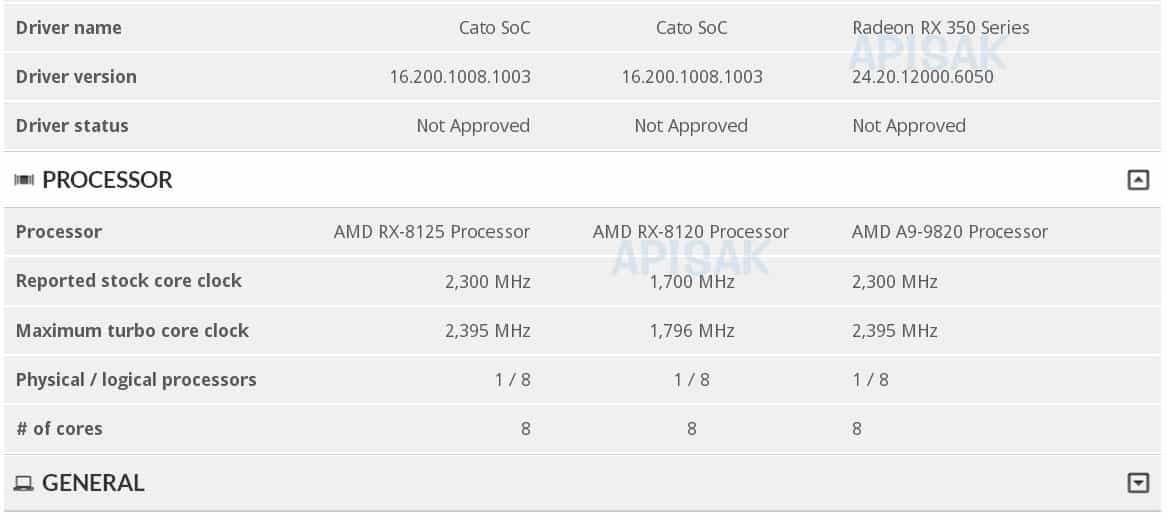
In short, AMD rebranded the Xbox One APU as a chip codenamed Cato and Chinese OEMs are now selling it for use in desktop PCs, but it actually seems that it was originally intended for embedded systems. Cato only emerged in 2019 in a screenshot of three SKUs’ specifications, but dates on my motherboard indicate that the APU was produced starting in 2014 and the chipset itself was produced in the end of 2015. The only available GPU drivers are based on version 17.12, which was released at the end of 2017. The GPU is reported as a 300-series part, which suggests a launch date around 2015. It’s hard to pin anything down for sure.
| The original leak from April 20192 |
|---|
 |
I can’t actually verify when or to whom this was released. AMD has kept quiet and sifting through their website has yielded nothing. A 2014 launch to enterprise customers makes more sense than a 2019 launch for mainstream PCs, but AMD refuses to let their old 28 nm cores die. Just last year in 2019 they released a new 1st-generation GCN GPU and two new Excavator APUs using years-old silicon.
I think the most likely possibility is a mix of these dates. AMD released an off-roadmap part around 2014 for embedded and industrial computers, but these computers are now being decommissioned and ending up in the hands of Chinese recyclers. Manufacturers in Shenzen are repurposing rather than destroying these embedded parts, and as of 2019 they are available in desktop PC motherboards.
What We Know
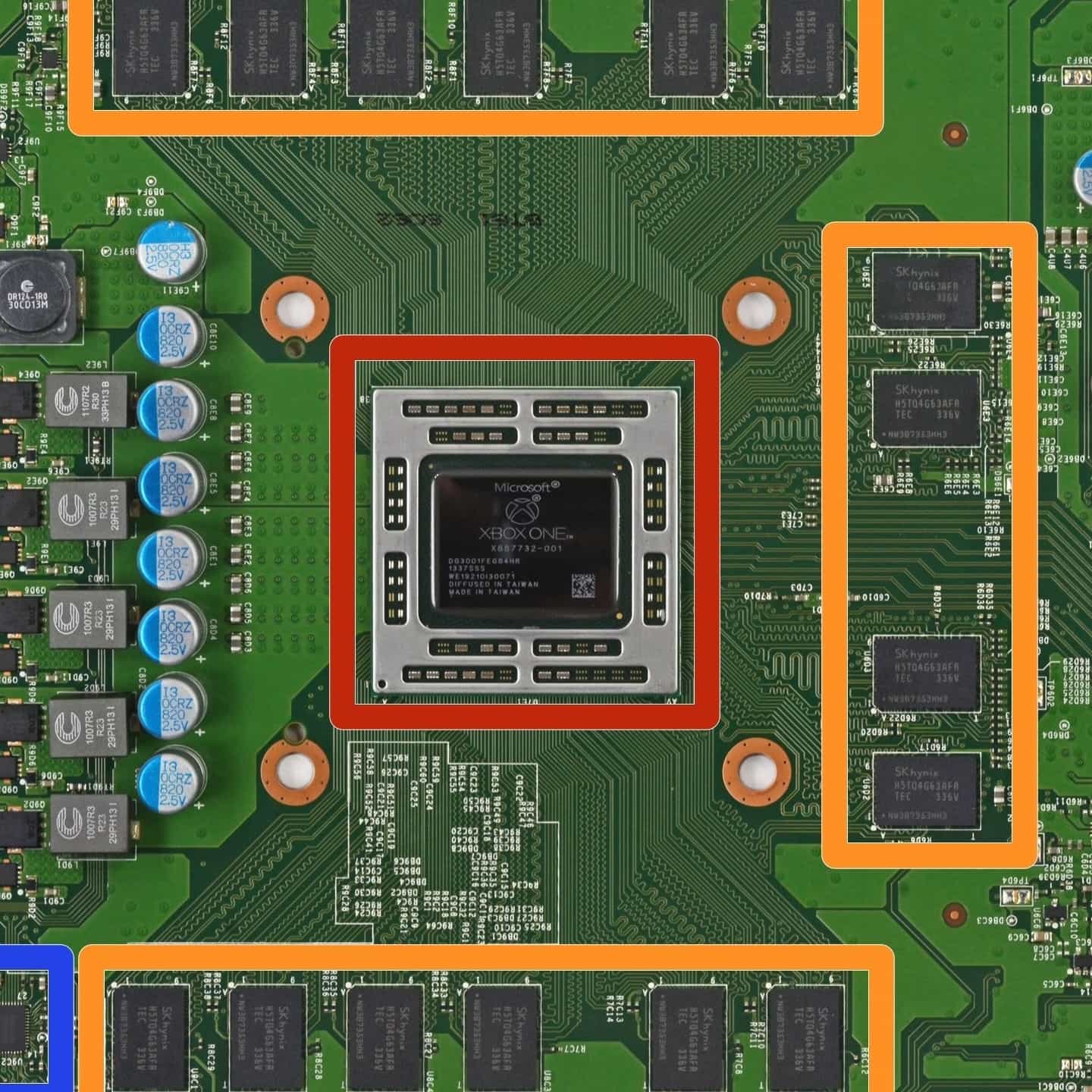
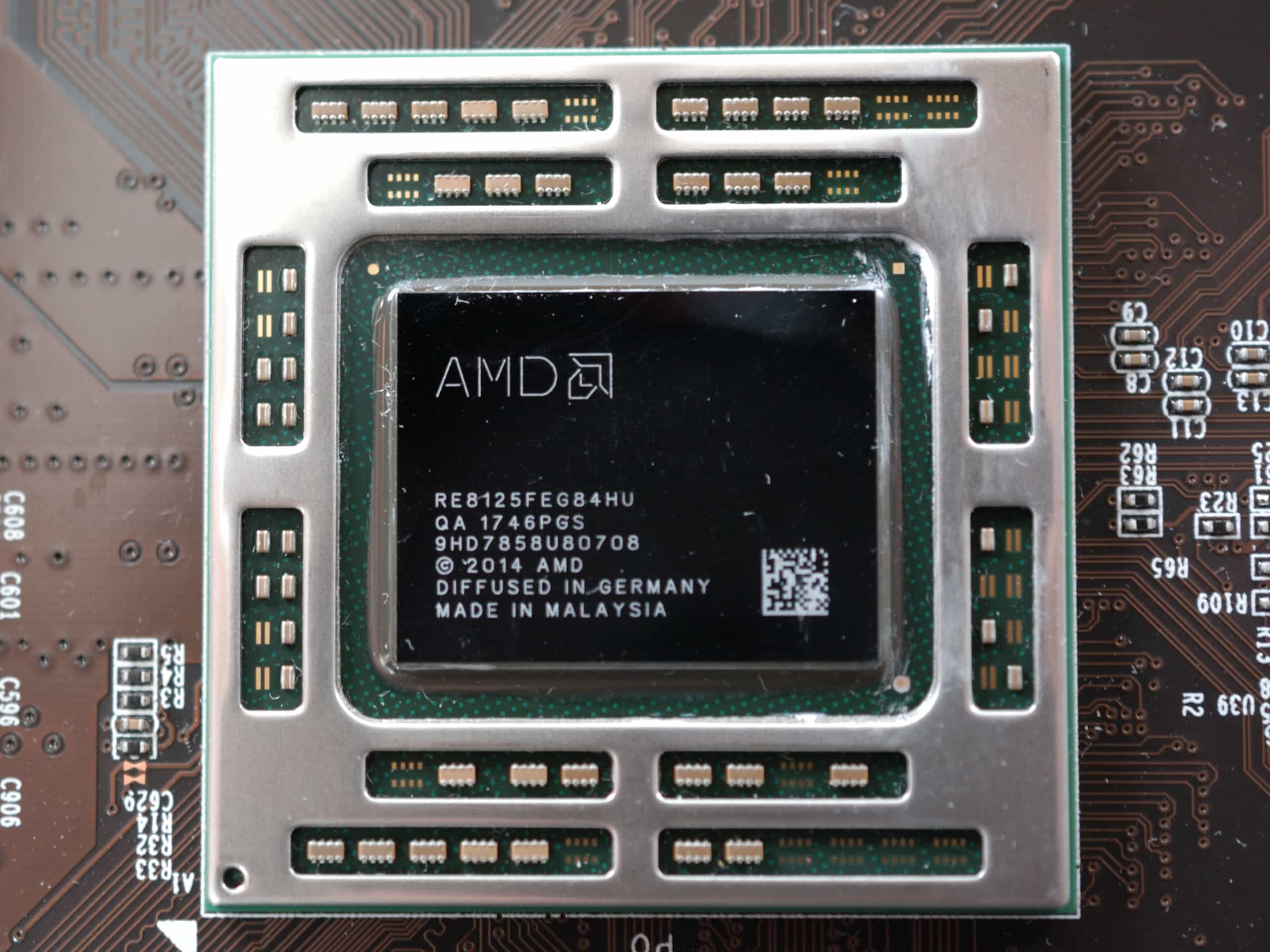
Cato is definitely the original 28 nm version of the Xbox One APU, itself codenamed Durango. Eyeballing the die next to my naked R9 280 (Tahiti-based, so 352 mm2) and making a couple sloppy measurments with my calipers indicates that the die is well over 300 mm2, which is consistent with Durango’s 363 mm2 area. The package also features a shim that looks identical to the 28 nm APU, because it is the 28 nm APU.
| A die shot of an Xbox One’s Durango APU from iFixit3 | A Cato APU, which is also the 28 nm Xbox One APU, because they are the same |
|---|---|
 |
 |
There are at least three motherboards in the wild using this APU, and it’s very likely that there are at least two more. The motherboard that I have was manufactured by Biostar according to the AliExpress listing, though this seems inaccurate.4 I believe that it was manufactured by Onda, a Chinese company infamous for some frankly bizarre cryptocurrency mining-oriented motherboards. Onda sells normal components for the most part, but the ones that make it to the West are a bit more… unique.
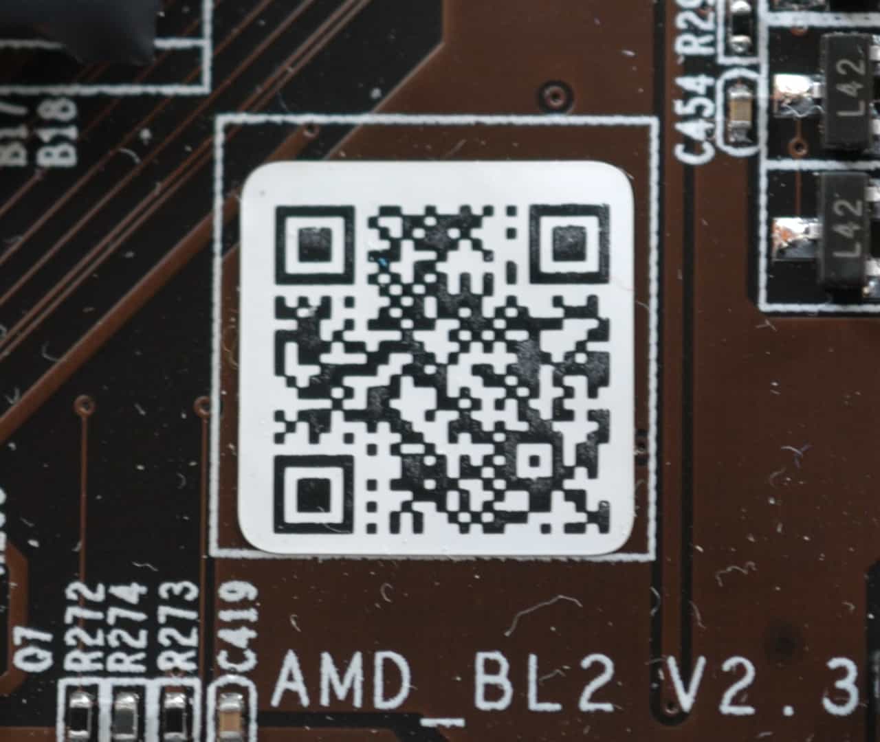
Model information for the motherboard is difficult to find, to say the least. Text silkscreened onto the board reading “AMD_BL2 V2.3” is below a QR code that returns the text “PG-00-11.A77.EAMDBL20V23010100/20GB2122/0803/0060.” The AliExpress listing names Biostar as the manufacturer, but this is probably incorrect.
| A QR code present on the motherboard | |
|---|---|
 |
 |
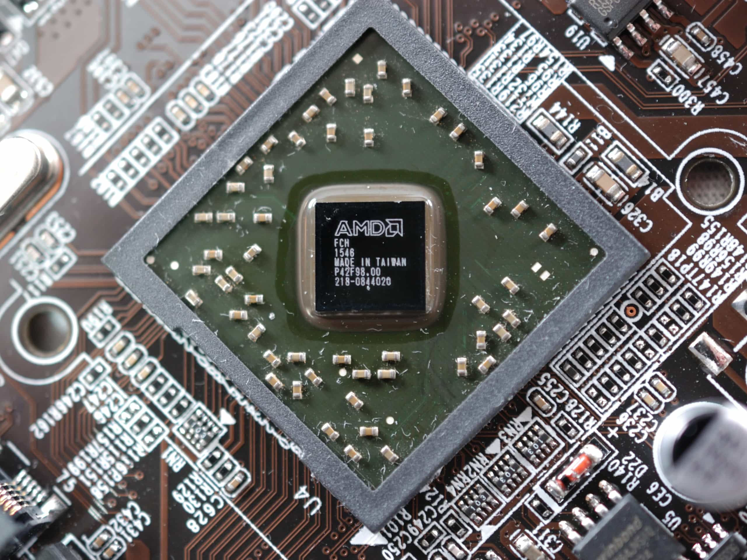
The QR code mentions the embedded A77E chipset, suggesting that this motherboard may have been designed as an embedded product first. However, the A77E die on this particular motherboard was produced in the 46th week of 2015, and my gut feeling is that it’s more likely that these chips are sourced from recyclers than from AMD’s mothballed warehouses. Seeing an NVMe-capable M.2 slot on an embedded motherboard from this period would also be unusual.
| The southbridge die featuring the date of manufacture |
|---|
 |
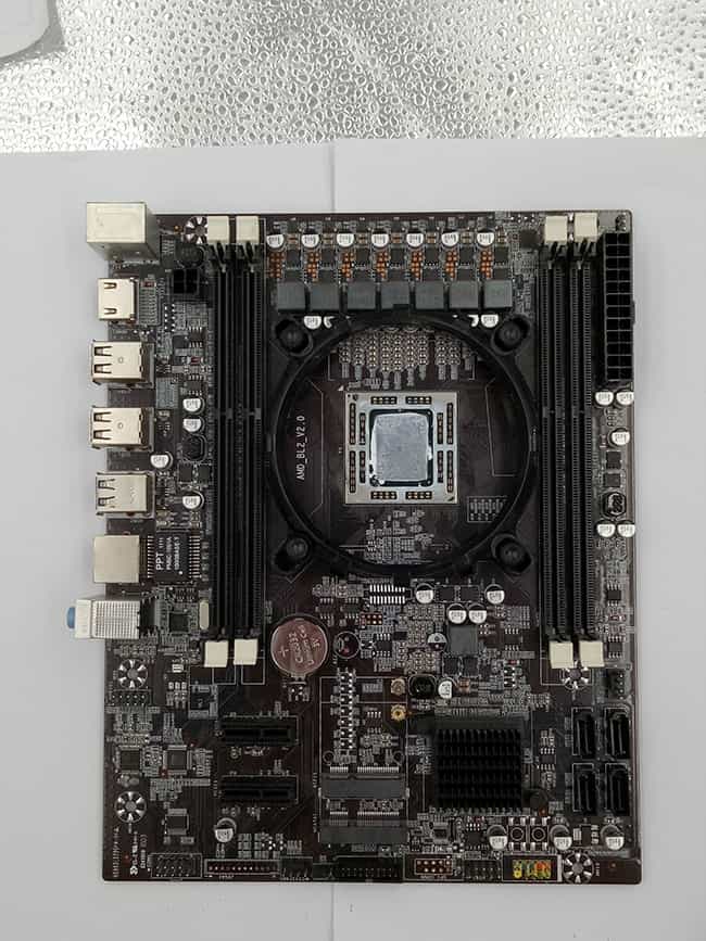
My motherboard is not the first version. According to silkscreening on it, it is version 2.3. Version 2.0 is shown below.
| An earlier version of a Cato motherboard. |
|---|
 |
There are tons of common design elements, from choice of passive components to layout and I/O variety. The expansion slots are different, though. Rather than one PCIe x1 slot and an M-keyed M.2 slot, this motherboard has two PCIe x1 slots, an mSATA slot, and a half-length Mini PCIe slot. Sadly, thermal paste on the APU obscures any markings. An additional VRM phase is present, but I don’t know for which bit of the APU.
If there exists a version 2.0 and a version 2.3, then it stands to reason that there are also versions 2.1 and 2.2, but I have not found any.
The third motherboard using this APU is found in a desktop PC released by Chinese OEM Chuwi. This PC, the AeroBox, uses a different motherboard.5 6 There is enough in common with mine and some other Onda motherboards that it’s highly likely to be another Onda design, perhaps a verion 3.0 of the two boards discussed already. It’s the same brown, and a lot of the layout and passives are similar, but it’s the least similar of the three.
| The Chuwi AeroBox after disassembly.6 |
|---|
 |
Like the others, there are two DIMM slots on each side of the APU and a Socket H mounting pattern for a cooler. The CMOS battery and buzzer are in the same locations, but the buzzer is actually populated on this motherboard. Only two SATA ports are present rather than four. An M-keyed M.2 slot is present, but rather than a PCIe x1 slot there is a short M.2 slot that appears to be E-keyed. This key is commonly used in wireless adapters like the present WiFi modem. Power delivery is somewhat different. An 8-pin EPS12V socket is present rather than a 4-pin ATX12V socket, and, like the earlier version of my motherboard, there are seven VRM phases. I honestly don’t know why since the APU can’t be overclocked.
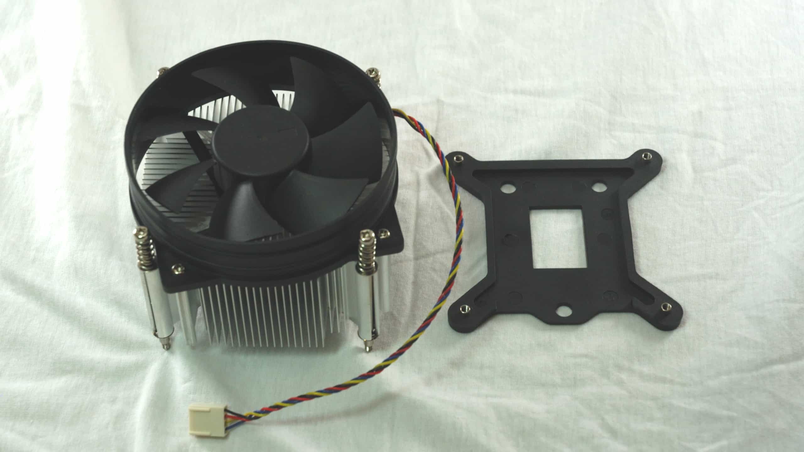
The use of a BGA package soldered to the motherboard actually introduces a small problem for use in a PC. Standard Intel Socket H mounting holes (i.e., LGA-115X and its 75 mm square pattern) are used, but Cato’s package is much shorter than Intel’s sockets. I tried to use a Corsair H55, but I could not get the waterblock tightened onto the die properly. The included cooler is a solid block of aluminium, but it’s chunky enough to handle Cato, albeit loudly.
| The basic stock cooler included with the motherboard. |
|---|
 |
Deciphering the Names
The CPU
The APU is codenamed Cato and the integrated GPU specifically appears to be codenamed Kryptos. There are several PCI IDs shared by components codenamed Cato, Kryptos, Anubis, Garfield, Garfield+, Arlene, and Pooky. I suspect that the other names, of which several are characters in the comic strip about the orange cat, are related to an implementation in the Xbox One and Xbox One S, but I cannot confirm this. Notably, there are no references to Durango, which is generally held to be the name of the Xbox One’s APU.7
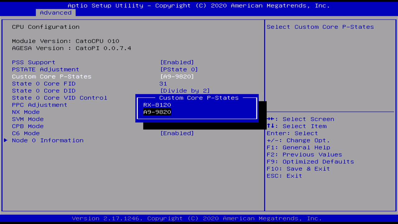
Cato has, or perhaps this motherboard lets it use, two different names. The AliExpress listing marketed it as an A9-9820, an A-series APU masquerading as a 9000-series Bristol Ridge part.
However, a setting in BIOS allows the APU’s named to be changed to RX-8120. Resemblance to the desktop FX-8120 is probably coincidental. RX branding may be more recognizable in graphics cards, but AMD actually used it first with embedded R-series APUs. These APUs used the same chips found in socket FM2 and FM2+ APUs. The first digit in their names refers to the number of cores.8 An embedded RX-8120 APU, then, contains eight CPU cores and is pretending to be some kind of Bulldozer-family APU.
The part number is printed on the die itself, revealing a third name and further confirming that Cato is rebadged Durango. The text “RE8125FEG84HU” is printed on the die. “R” indicates that this APU is an R-series part and “E” indicates that it is intended for embedded systems. “8125” translates to a product name, RX-8125. The remaining characters are shared with corresponding text printed on Durango barring the last letter. Durango uses the part number “DG3001FEG84HR” instead.3
Referring back to the first screenshot of Cato,2 the RX-8125 and A9-9820 share a clockspeed. This in conjunction with the RX-8125 name hinted at on my APU’s die makes me suspect that it is an RX-8125 and the A9 branding came later, perhaps for Chuwi specifically, but this is speculation.
Integrated GPU
These leaks also mention an integrated GPU branded as the RX 350. RX 350 is a somewhat anachronistic name. It combines the RX branding introduced for GPUs in the 400 series with a 300-series part. It is a 2nd-generation GCN GPU based on Bonaire, which was originally released in the HD 7790 in 2013. The GPUs in both the Xbox One and PlayStation 4 are derived from this chip.
Several sources have called this GPU an R7 350 and some have gone further and published performance estimates based on this name, which are all wrong, because this is definitely not an R7 350. The R7 350 is a real graphics card, containing either an Oland or a Cape Verde chipset, but it’s a desktop PCIe add-in card and absolutely not an integrated GPU. The confusion seems to originate from marketing material published by Chuwi for the AeroBox, which erroneously claimed that the PC contained an R7 350.4 5 Performance benchmarks discussed later prove that the RX 350 used here is not Cape Verde and definitely not Oland. Kryptos also has a PCI device ID of 154C while Oland and Cape Verde variants have IDs in the 6000 range.
Specifications
The APU Itself
Despite AMD recycling a lot of existing designs and logic into a new floorplan, Durango is a unique APU. For instance, it’s AMD’s first processor with quad-channel memory in a single NUMA node, more than any AMD processor until the release of 2nd-generation Epyc. It was AMD’s first processor to feature a platform security processor that’s now common on most of their processors, though that’s beyond the scope of this article. It was AMD’s first monolithic 8-core CPU, a feat that would not be repeated until the launch of their Arm-based Opterons a couple years later. Cato, being nothing more than rebadged Durango, shares most of these traits.
| Comparison of 28 nm APUs | |||
|---|---|---|---|
| Cato | Athlon 5350 | A10-7870K | |
| Microarchitecture | Jaguar | Jaguar | Steamroller |
| Cores/Threads | 8/8 | 4/4 | 2/4 |
| CPU Clock (Turbo) | 1.75 GHz or 2.35 GHz (n/a) | 2.05 GHz (n/a) | 3.9 GHz (4.1 GHz) |
| GPU Architecture | 2nd-gen GCN | 1st-gen GCN | 2nd-gen GCN |
| Compute Units | 12* | 2 | 8 |
| Max. GPU Clock | 985 MHz** | 600 MHz | 866 MHz |
| Memory Channels | 4* | 1 | 2 |
| Memory Speed | DDR3-2133** | DDR3-1600 | DDR3-2133 |
| TDP | 135 W** | 25 W | 95 W |
| *Determined from benchmark results | |||
| **Unconfirmed and taken from AeroBox marketing material | |||
| A table comparing several APUs from the early 2010s. | |||
Cato contains two quad-core blocks of Jaguar cores, giving it eight in total. The quad-core blocks behave similiarly to separate processors, or perhaps the two dies in a Core2Quad or two CCXes in an early Ryzen CPU. An entire block’s core frequencies and voltages change about simultaneously going by their behavior in HWiNFO64.
These Jaguar cores do not feature SMT, because of course they do not feature SMT, because they are Jaguar cores. There is no L3 cache available to them, and each block has 2 MiB of L2 cache shared by its four respective cores. The eSRAM contained in the die appears to be unavailable, is not used as L3 cache, and is absolutely not used as L4 cache.
Like the GPU’s name, some of this confusion can be blamed on Chuwi. Chuwi’s marketing claims that this APU has 8 MiB of L2 and L3 cache, which is simply wrong. It has a total of 4 MiB of L2 and zero MiB of L3.
That is because, and I cannot emphasize this enough, this is a rebranded Xbox One APU.
As mentioned before, the name of the CPU can be changed in a BIOS setting. There is some significance to the choice. If configured as an RX-8120, the APU runs at up to 1.75 GHz and requires 1.2 V at this speed. If configured as an A9-9820, the APU runs at up to 2.35 GHz and 1.4 V instead. This configuration in theory consumes 83% more power while only increasing the frequency by 34%, but frankly there’s little reason to not use the faster setting given how slow and efficient Jaguar is. This isn’t a particularly power-hungry system anyway. Perhaps coincidentally, the RX-8120 shares a clockspeed with the Xbox One itself.
The GPU is most similar to Bonaire, but it was modified to meet Microsoft’s requirements. These don’t really touch the underlying GCN architecture, though. Although Durango only used 12 compute units, die shots revealed that two were disabled in order to ensure higher yields, and GPU-Z reports that all 14 are enabled in Cato. I disagree with that and believe that, like the Xbox One, only 12 compute units are enabled. This will be discussed in the benchmarks section.
Integrated GPUs are usually starved for memory bandwidth, and Cato is no exception. Cato’s maximum memory bandwidth is 68 GB/s thanks to its quad-channel memory, but this motherboard only supports memory speeds up to DDR3-1866, dropping the maximum to 60 GB/s. This is still incredibly fast for an APU, but it’s shared by the CPU and GPU and it’s substantially lower than a basic graphics card. A discrete R7 260 on the other hand comes with GDDR5 standard, giving it 96 GB/s of bandwidth all to itself. Limited bandwidth is a major issue with high-end APUs in general. In some games, the framerate increases nearly linearly with memory clock when using Kaveri’s integrated graphics, for example.9
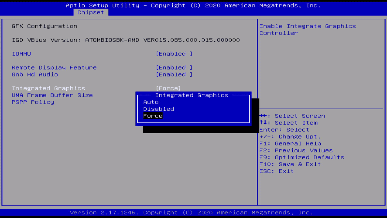
By default, only 512 MiB of memory is allocated as VRAM, and at first glance there is no option to change this setting in the “GFX Configuration” menu. Even without a separate PCIe graphics card in the system, the integrated graphics must be set to “force” rather than “auto.” This presents a menu that allows up to 2 GiB of memory to be allocated as VRAM, which is what most Bonaire graphics cards shipped with. Allegedly, there is a BIOS floating around in the wild that does not contain this setting at all, but my source is a YouTube man who was extremely wrong about a lot of aspects of Cato and Kryptos and this motherboard. The BIOS version string containing “CatoBDK” leads me to believe that it’s be a beta build, though, to say nothing of the BIOS options that correspond to ports that are not wired or options that outright brick the system.
Contrary to the AliExpress listing,4 Cato supports quad-channel memory and more importantly the motherboard is actually wired for it. Firmware readouts show references to memory channels A, B, C, and D, and memory performance is consistent with quad-channel operation. Internally, Cato contains a cache-coherent link between the CPU cores and the memory controller and northbridge. Microsoft that this link’s throughput is 30 GB/s,10 and this appears to be accurate albeit misleading. I believe that this is actually a full-duplex link that is 15 GB/s in each direction rather than a 30 GB/s half-duplex link. Again, this will be discussed in the benchmark section. The GPU meanwhile has access to the full memory bandwidth.
Chuwi’s marketing material claims that this APU has a 135 W TDP, and napkin math suggests that this is plausible: 25 W for an Athlon 5350, double it because it has double the cores, then add 95 W for an R7 260 but subtract 10 W because it doesn’t have any GDDR5.
The Rest of the Platform
Cato has just one video output and five PCIe lanes total. The video output may be hooked up to an HDMI port (this motherboard) or a DVI port (the AeroBox). Meanwhile, a PCIe x4 link acts as the southbridge downlink and a PCIe x1 link connects the gigabit Ethernet controller; this is also true of the Xbox One itself. This system eschews the custom Xbox One southbridge though and instead uses a standard Bolton-based chipset. This motherboard is using the embedded A77E specifically, which is essentially identical to the desktop A78 chipset introduced alongside socket FM2+. This chipset controls all SATA and USB ports in addition to the user-accessible PCIe lanes, which run at PCIe 2.0 speeds.
There are only two expansion slots available. There is a PCIe x1 slot, and there is an M.2 slot that supports booting from NVMe storage. Bolton chipsets have four PCIe lanes for connecting general-purpose devices, and a BIOS option defaults to splitting them three ways into a x2 link and two x1 links. The x2 link is routed to the M.2 slot while one x1 link is routed to the PCIe slot and the other x1 link seems to disappear into the aether. A BIOS option exists to modify how the lanes are configured, and notably one option creates a single PCIe x4 link, presumably to the M.2 slot alone to maximize NVMe storage performance. This option is completely broken and the system fails to POST if it is changed from the default and will require a BIOS reset, so you’re stuck with a blazing fast 1 GB/s if you want to use NVMe storage.
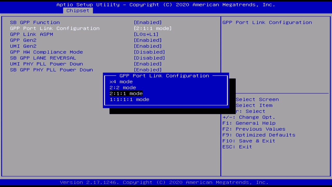
The M.2 slot also accepts SATA SSDs, but I personally have not verified this as I lack the hardware needed. The method used to switch the bus type is something of a bodge. Rather than a BIOS setting, there are four jumpers near the M.2 slot that can be set to SATA or NVMe mode. I assume they connect to the four sense pins in the M.2 slot that indicate which type of device is installed, but I couldn’t find any continuity using my multimeter. A77E supports six SATA ports, so I assume that this is a separate fifth port and is not shared with the four normal SATA ports; again, this is an assumption.
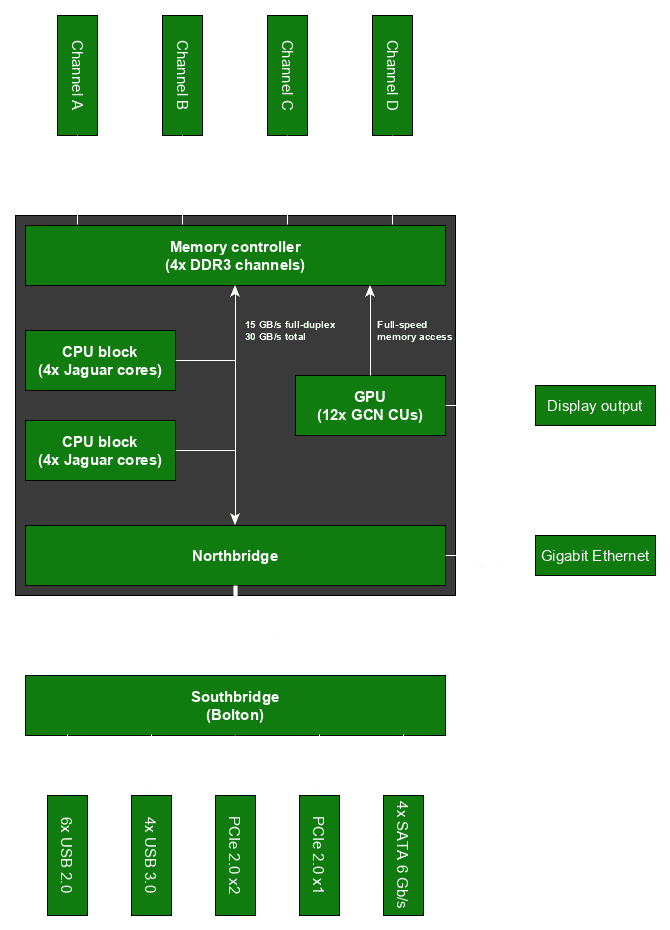
tl;dr, the parts of the APU and motherboard that you as an end user probably care about look something like this:
| A block diagram of the motherboard and the APU itself. |
|---|
 |
There are a few other bits and pieces of interest. Two PWM fan headers are present, one for a case fan and the other for the heatsink fan. An IT8772E super I/O chip is present and provides PS/2 ports, sensors, and a header for a serial port. This little chip is an extremely important part of what makes this PC a PC. Several solder pads are present and labeled for JTAG, a SPI bus, and an onboard buzzer, but these are unpopulated and are probably leftovers from development.
That’s all I can think of that seems interesting. Send me a message if there are any more details you’d like to know about. Definitely send me a message if I made a mistake here, but please give me some solid evidence because there is a lot of misinformation about Cato out there from ostensibly trustworthy people and media outlets who simply do not understand what they are talking about or looking at.
Benchmarks and Analysis
“[T]he performance test of the onboard CPU can almost match the performance of the i5 7400.,”4
Look, all I can say going in is not to get your hopes up. It’s bad. It’s really bad. Like, I’ve overclocked an Athlon 5350 before and use it on purpose in my desk PC and I was still disappointed.
Let’s consider Cinebench to put it in perspective. In Cinebench R15, Cato at its highest frequency scores 378 points in the multithreaded benchmark or, when clocked down as an RX-8120, 288 points. Ryzen 5000 series CPUs score within spitting distance in the singlethreaded benchmark, reaching around 260 to 280 points. So if you opt to use the slower RX-8120 configuration, the entire APU scores maybe ten points higher than a single Zen 3 core, and that’s without leveraging SMT for an extra 20ish% performance for free.
I see no reason to run the full gamut of benchmarks. Nobody is using this except as a novelty. But we know how it performs anyway thanks to Intel.
Around the time AMD released Jaguar, Intel released their competing low-power Silvermont microarchitecture. Overall, the two cores are roughly equivalent, though Silvermont-based CPUs generally win in benchmarks since Intel actually bothered to implement turbo boost.
Unlike AMD, Intel didn’t just use their low-power core for cheap client systems. Intel released Avoton CPUs with eight Silvermont cores for embedded servers and telecommunications. Since these, like Cato, have eight cores, and since Jaguar and Silvermont are approximately the same, then by the transitive property Avoton is equivalent to the CPU portion of Cato. You want to know how this thing performs as a general-purpose desktop processor? Then go look up Atom C2750 benchmarks. We’ve known how the Xbox One APU would perform in a PC for seven years because we’ve had Atom C2750 benchmarks for seven years. It’s not good. Multithreaded performance compares to contemporary A8 and A10 APUs or to Core i3 CPUs. Singlethreaded performance is abysmal.
There are only a few interesting benchmarks to discuss: c2clat, a core-to-core latency benchmark; AIDA64’s cache and memory benchmark; and AIDA64’s GPGPU benchmark. These reveal information about the APU itself and support some of the claims I made in the previous section.
Core-to-core Latency Using c2clat
c2clat11 is a simple tool that measures latency between cores by compiling a C++ program. While I admittedly am unsure if the results are quantitatively accurate, I’m confident that they’re qualitatively accurate. Ten runs were averaged on the A9-9820 itself in addition to an Athlon 5350 and an A10-7870K. The Athlon 5350 was locked to 2.1 GHz and the A10-7870K was locked to 3.9 GHz; this tool is sensitive to dynamic clockspeeds and locking the frequency reduces variation between runs.
Two charts are presented for each APU: one with the average time, and one with the approximate number of clock cycles. These ranges were obtained by multiplying the average time by the clockspeed and adding or subtracting one standard deviation and rounding to the nearest integer. In certain cases, all runs of the benchmark returned the same time. In this case, the range is obtained by adding or substracting half a nanosecond. The “near” core pairs are shown in blue while the “far” core pairs are shown in red.
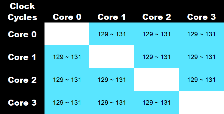
| The core latency of a Cato APU in terms of time | The core latency of a Cato APU in terms of clock cycles |
|---|---|
 |
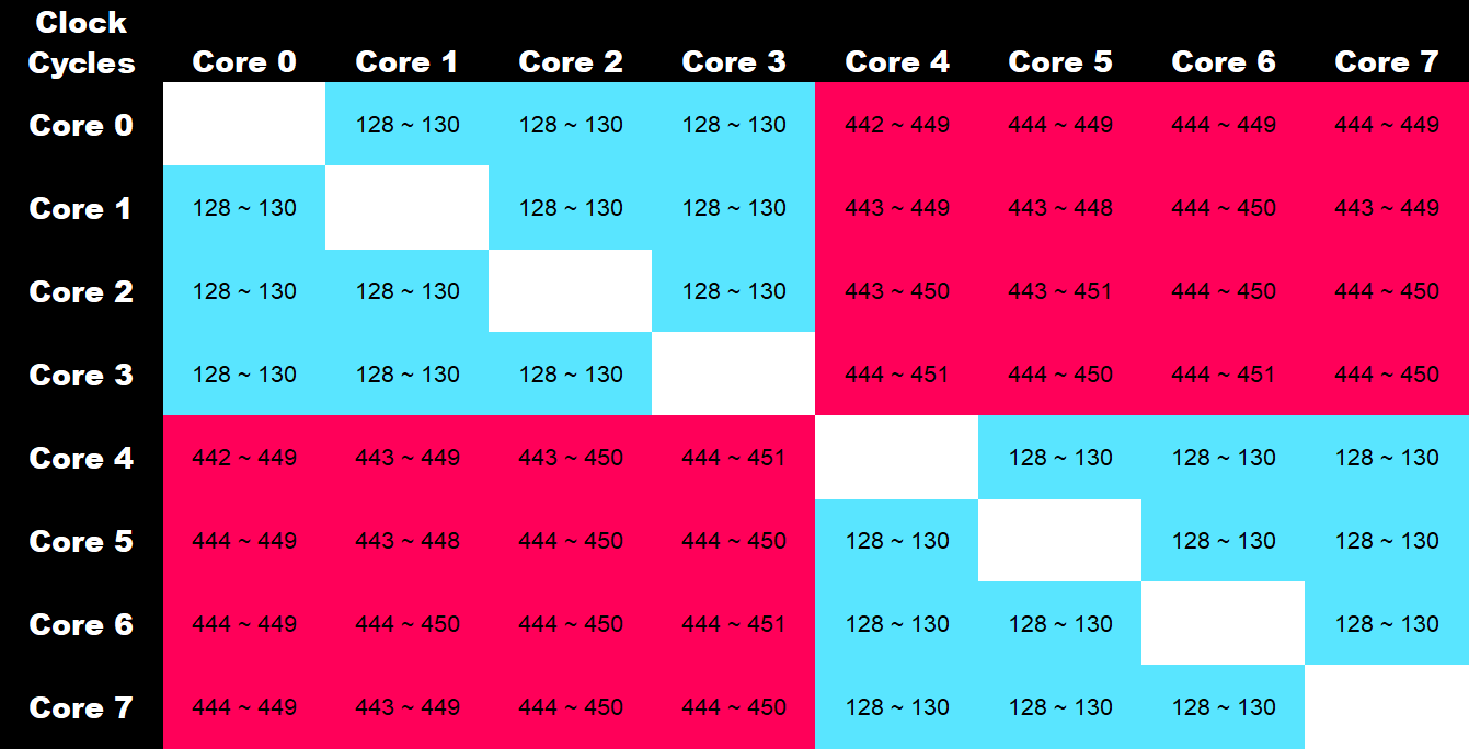 |
The latency between any two near cores is 55 ns, which works out to about 130 cycles. Latency between far cores is substantially higher at nearly 200 ns or 450 cycles. It takes about three and a half times as long to access a core in the other quad-core block, which is reasonable given that this design was probably never intended to scale beyond four cores and we’re practically looking at a dual-socket system in a chip.
| The core latency of a 2.1 GHz Athlon 5350 in terms of time | The core latency of a 2.1 GHz Athlon 5350 in terms of clock cycles |
|---|---|
 |
 |
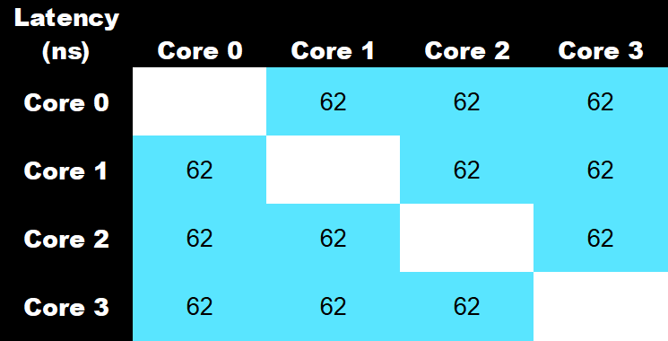
All four cores in the Athlon 5350 are equidistant. Kabini is just a boring ol’ quad-core CPU. Latency is a bit higher than Cato’s near cores, but this is due to the frequency deficiency. Once converted to clock cycles, the ranges overlap. The Athlon 5350’s upper and lower bounds are both one cycle higher, but that is purely due to rounding and there is no meaningful difference.
| The core latency of a 3.9 GHz A10-7870K in terms of time | The core latency of a 3.9 GHz A10-7870K in terms of Clock cycles |
|---|---|
 |
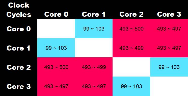 |
As a descendent of Bulldozer, the A10-7870K features two modules featuring two cores each. Latency is much higher when accessing a different module, taking nearly five times as long! Honestly, I’m not convinced that this is completely accurate, but Bulldozer was such a bad architecture that I’m willing to believe it.
Converting the time to clocks suggests something profound. Even though AMD recycled an existing CPU design and didn’t make something bespoke for Microsoft, and even though AMD probably never intended the design to scale beyond four cores, Durango and later Cato are penalized less while accessing cores that they were never meant to than the grandchild of a microarchitecture that was designed around parallel processing is penalized when doing the one thing at the heart of its design philosophy.
Admittedly, I’m assuming that comparing c2clat results across microarchitectures is valid, but again, it’s Bulldozer. Is it really unbelievable that even a couple of glued-together tablet SoCs are better?
AIDA64’s Cache and Memory Benchmark, Minus the Cache
Three sets of results are shown using two and four DIMMs set to DDR3-800 and four DIMMs set to DDR3-1600. DDR3-800 is the slowest I can set the memory to run at and DDR3-1600 is the fastest I can get the system to boot at.
In memory read, the DDR3-1600 configuration nearly reaches 15 GB/s, while the DDR3-800 configuration is a bit slower at 14.5 GB/s. When using two DIMMs rather than four, the DDR3-800 configuration only reaches 11.6 GB/s. This reveals two important things about Cato’s memory system.
| Read (GB/s) | Write (GB/s) | Copy (GB/s) | Latency (ns) | |
|---|---|---|---|---|
| DDR3-800 (2x) | 11.6 | 8.8 | 9.8 | 132 |
| DDR3-800 (4x) | 14.5 | 9.4 | 15.8 | 135 |
| DDR3-1600 (4x) | 14.9 | 9.4 | 17.6 | 123 |
| Determining the memory configuration using benchmarks. | ||||
The two-DIMM DDR3-800 memory read benchmark reaches 90% the maximum theoretical throughput of a dual-channel configuration, which is 12.8 GB/s. This is typical for this benchmark. The four-DIMM test exceeds this limit, proving that the system does indeed operate in quad-channel mode. But this quad-channel result is significantly slower than the theoretical limit of 25.6 GB/s, and despite doubling the memory speed, the four-DIMM DDR3-1600 memory read benchmark is barely faster. Both benchmarks seem to hit a ceiling at about 15 GB/s.
This behavior is definitely due to the 30 GB/s link,10 but the memory read benchmark alone is insufficient to explain why. Instead, let’s look at the memory copy results. At 15.8 GB/s and 17.6 GB/s, these are somewhat lower than twice the memory write results but importantly are both faster than 15 GB/s, demonstrating that this 15 GB/s ceiling is real but can be exceeded in mixed read/write workloads.
AIDA64 calculates bandwidth in this benchmark using the STREAM convention. The result is calculated by dividing the total amount of data transferred across the memory bus in both directions by the time taken.12 To summarize, a piece of data is read, then it’s written back elsewhere, and since that’s two operations, the convention counts the total amount of data transferred across the memory bus as the size of the piece of data times two. These results are consistent with a stream of data being read and then written at about 8 or 9 GB/s each, which is expected given that the memory write speed is slower and acts as a bottleneck.
It’s up for debate whether or not the STREAM convention is the ideal metric, but that’s beside the point. What matters here is understanding that this Cato APU was not able to exceed 15 GB/s in a pure read workload due to an internal limitation. However, it was able to simultaneously read and write more than 15 GB/s in a mixed workload, with each direction handling at least 8 GB/s for an aggregate 16 GB/s going through the pipe at any time. It only makes sense that Cato can exceed the 15 GB/s ceiling under certain conditions if the internal 30 GB/s link is indeed a full-duplex link whose nominal throughput is the sum of each direction.
Note that this link speed is unaffected by CPU or memory clock. My best guess is that this is a full-duplex 128-bit bus clocked at 933 MHz, or 133 MHz with a 7x multiplier (give or take small fluctuations in the system’s clockspeeds). This is consistent with an estimate made by SemiAccurate.13
Somebody Else’s GPGPU Benchmark
I cannot get the drivers to work.
Not in Windows 7 anyway. Any workload beyond a basic 2D Windows desktop causes the system to lock up. DirectX, OpenGL, OpenCL, whatever. I tried installing Windows 10 and the system refuses to boot now, let alone install GPU drivers. I’m taking these results from Twitter user @brutuscat2 instead because I literally cannot do anything with the graphics.
Most of the AIDA64 GPGPU benchmark suite can be ignored. I only care about one benchmark here because working backwards from that result should produce a good estimate of the GPU’s illusive core clock.
| A screenshot of @brutuscat2’s benchmark results posted to Twitter.14 |
|---|
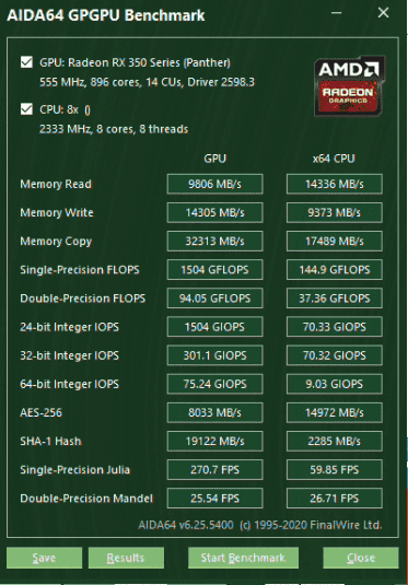 |
(Well, actually, one last note about the memory system. The GPU slightly exceeded 30 GB/s in the memory copy benchmark, verifying that it is indeed able to access the system memory at full speed unlike the CPU.)
Brutus’s GPU scored 1504 GFLOPS in this test, and at the very least this is enough to disprove the notion that this is anything smaller than Bonaire. This particular value for a couple of GCN graphics cards that I tested that do report core clocks is nearly equal to the number of shaders times the number of gigahertz times two (each shader can do one fused-multiply-add per clock, which counts as two floating point operations). If we take the known floating-point performance and possible amounts of shaders, then we should be able to get the core clock. Take a look:
| Chipset | CUs | Required clock @ 1504 GFLOPS |
|---|---|---|
| R7 350 (Oland) | 6 | ~1958 MHz |
| R7 350 (Cape Verde) | 8 | ~1469 MHz |
| Xbox One | 12 | ~979 MHz |
| Kryptos (reported) | 14 | ~839 MHz |
| Determining the GPU's core clock from FP32 performance. | ||
It’s very clear that the GPU is not Cape Verde and is absolutely not Oland. AMD would simply never clock a 28 nm GCN GPU that high. The maximum stock core clock used by any of them including space heaters like Grenada and Fiji was 1050 MHz. It wouldn’t be until Navi two process nodes and four microarchitectures later that AMD would be willing to ship anything guaranteed to run at the core clock Oland would require here.
So we’re left with the Bonaire equivalents. With 12 compute units enabled, the GPU needs to run at nearly 1 GHz, which by this point in 28 nm GCN’s life cycle is trivial. But this is an APU, so memory bandwidth limits performance and a wider-but-slower core can be configured to reduce power consumption and thus cooling requirements, a tactic implemented effectively by the R9 Nano. Since there’s no tool to measure the core clock, it’s a toss-up, right?
| Marketing material from Chuwi describing the AeroBox’s GPU5 | A screenshot of Radeon settings showing the GPU clock.15 |
|---|---|
 |
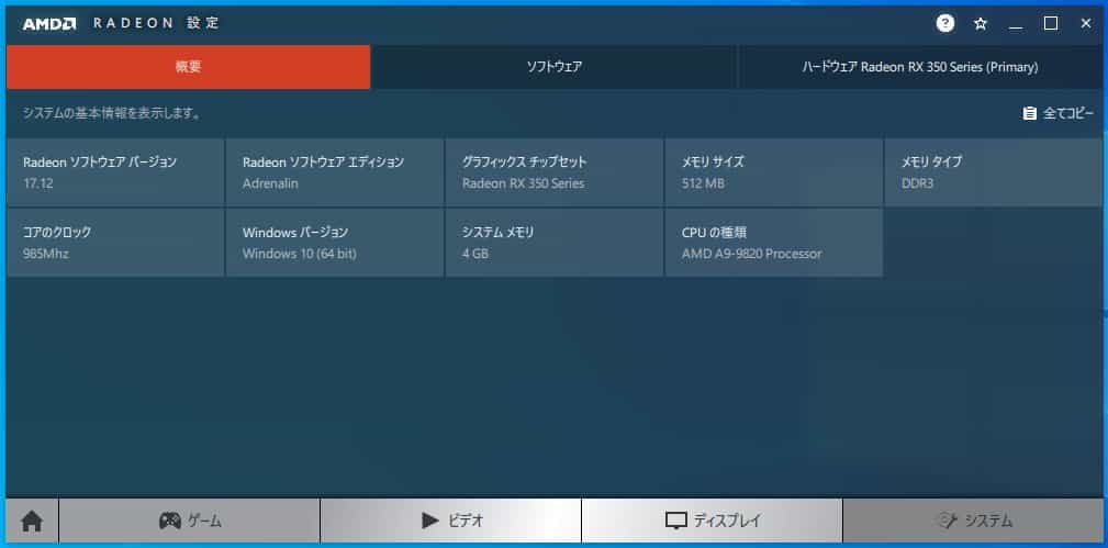 |
Not quite. Both Chuwi’s marketing, despite all its flaws, and Radeon settings claim that this GPU has a maximum core clock of 985 MHz. Quite literally no other GCN GPU boosts to that precise frequency if Wikipedia is to be trusted. If that clock can be sustained for the duration of the GPGPU benchmark suite, then that’s our configuration. AMD did not enable any additional compute units; Cato has 12 compute units enabled just like Durango.
And I can’t blame them. This literally is the Xbox One APU. I have no doubt that AMD changed a single manufacturing step while making these, and that’s making a huge assumption because AMD could very well have found a box of these die in a warehouse and decided to sell them to somebody.
Conclusion
Please do not buy this. Maybe as a display piece but nothing more than that. This is ewaste. AMD was right to never release Durango in a PC. Performance is mediocre. We’ve known it’s mediocre. We saw how the Xbox One did, we saw how Kabini with discrete graphics did, we saw how Avoton did. Even the really cool misinformation that insists this an Excavator-based APU with four modules or a special Jaguar variant with SMT would have resulted in a whole lot of R&D budget dedicated to mediocrity. I waited nearly 20 minutes waiting for one Cinebench run and realized that I just can’t be bothered to dedicate the energy to a full benchmark suite. The Xbox One and Avoton may not have been fast, but at least they had a purpose.
And the worst part? People are buying this. People are buying this motherboard to use it in actual computers. Actual office machines, actual HTPCs, hell, even actual gaming rigs! The AliExpress listing had about 120 units available when I ordered and when I checked earlier while writing this analysis it had dropped to 60 units. I personally know of three others who have bought them, but we all knew what we were getting into. Sketchy marketing for a SKU that’s only in two things available only from a country halfway around the world should raise so many red flags for the average buyer, but Reddit and the Linus Tech Tips forums are littered with threads speculating that this might be a hidden gem that AMD doesn’t want you to know about. I mean, eight cores for just $125? There’s no way it can possibly be slower than an Athlon 3000G plus motherboard that has a warranty and customer service and also costs less! Even worse, there are tech support threads because again I cannot emphasize this enough people ignored the red flags and actually bought the damned thing and need help getting it to work.
This isn’t a hidden gem. There is no diamond in the rough here. This APU was never designed to be used in a PC and it was a mistake to make a PC that uses it. The A9-9820 is only interesting because it was used in something else first.
Sources
- ShrimpBrime. “IPASON A9-9820 Mobo AMD_BL2 V2.3.” Linus Tech Tips Forum. Nov. 15, 2020. Accessed Dec. 5, 2020. Live: https://linustechtips.com/topic/1268937-ipason-a9-9820-mobo-amd_bl2-v23/, archive: https://archive.is/rvogr [return]
- TUM_APISAK. “RX-8125, RX-8120, A9-9820+RX 350.” Reddit. Apr. 6, 2019. Accessed Dec. 15, 2020. https://www.reddit.com/user/TUM_APISAK/comments/ba05ec/rx8125_rx8120_a99820rx_350/ [return]
- “Xbox One Teardown.” iFixit. Nov. 21, 2013. Accessed Dec. 15, 2020. https://www.ifixit.com/Teardown/Xbox+One+Teardown/19718 [return]
- “AMD A9-9820 8-core Desktop APU R7 350 GPU With Motherboard ComboSupport DDR3 2.35GHz Compared with i5 7400 High Performance Set.” AliExpress. Accessed Dec. 5, 2020. Live: https://www.aliexpress.com/item/1005001340237782.html, archive: https://archive.is/iAK28 [return]
- “AeroBox High Performance Office Mini PC.” Chuwi. Accessed Dec. 5, 2020. Live: https://www.chuwi.com/product/items/Chuwi-AeroBox.html, archive: https://archive.is/VCrkM [return]
- “Chuwi AeroBox Real Machine Review.” Win-Tab. Machine translation via Google Translate. Oct. 14, 2020. Accessed Dec. 15, 2020. https://win-tab.net/imported/chuwi_areobox_review_2010142/ [return]
- “Advanced Micro Devices, Inc.” Device Hunt. Accessed Dec. 15, 2020. https://devicehunt.com/view/type/pci/vendor/1022/ [return]
- “AMD Embedded R-Series Family.” AMD. Accessed Dec. 5, 2020. Live: https://www.amd.com/en/products/embedded-r-series, archive: https://archive.is/yaNJu [return]
- Martin, Ryan. “Memory Scaling on the AMD Kaveri A10-7850K APU.” eTeknix. March 2014. Accessed Dec. 15, 2020. https://www.eteknix.com/memory-scaling-amd-kaveri-a10-7850k-apu/7/ [return]
- Sell, John and Patrick O’Connor. “Main SoC and Xbox One Kinect.” Hot Chips 25. Aug. 26, 2013. Accessed Dec. 15, 2020. https://old.hotchips.org/wp-content/uploads/hc_archives/hc25/HC25.10-SoC1-epub/HC25.26.121-fixed-%20XB1%2020130826gnn.pdf [return]
- Rigtorp, Erik. “c2clat.” GitHub. Oct. 8, 2020. Accessed Dec. 15, 2020. https://github.com/rigtorp/c2clat [return]
- Fiery. “Memory Bench Questions.” AIDA64 Forum. Jan. 9, 2017. Accessed Dec. 5, 2020. Live: https://forums.aida64.com/topic/3708-memory-bench-questions/, archive: https://archive.is/he1qe [return]
- Demerjian, Charlie. “A Deep Dive into Microsoft’s Xbox One’s Architecture.” SemiAccurate. Aug. 29, 2013. Accessed Dec. 15, 2020. https://semiaccurate.com/2013/08/29/a-deep-dive-into-microsofts-xbox-ones-architecture/ [return]
- brutuscat2. Tweet. Nov. 17, 2020. Accessed Dec. 5, 2020. [Live: https://twitter.com/brutuscat2/status/1328798180654387203, archive: https://archive.is/s9vpQ] [return]
- momomo_us. Tweet. Nov. 8, 2020. Accessed Dec. 11, 2020. Live: https://twitter.com/momomo_us/status/1325412901868367873, archive: https://archive.is/eut7e [return]

Technical Writer & Gamers Rise Up Enthusiast
Bottom Text