
How To Write Small and Do Other Things Small - Part 1 - Lithography
Published:
by:
Moshe Dolejsi
Estimated reading time: ~7 minutes
What’s the motivation to create smaller features? Is it raw speed? Performance?
While you’re thinking about that get a piece of paper and draw as many squares on it as you can (No adjacent squares can touch). Each square is a transistor and every 4 transistors is a chip and by the way I’ll give you 100 bucks per chip, and oh yes the answer is money. Lots of money.
Warning : This is by no means going to be an all-encompassing dive into the nitty gritty details of fabrication, for that I’d recommend the excellent online course, “Chemical Processes for Micro- and Nanofabrication” (free) taught by Chris Mack.
Squares might be a simple way to think about transistors but if you zoom in really close it turns out almost every modern chip consists of sets of parallel lines up and down, and then occasionally parallel lines left and right as is shown in a representative CMOS NAND layout (figure 1).
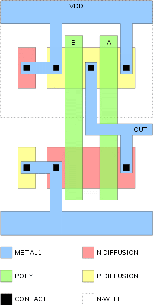
Think of the blue as sitting on top of everything else with the black contacts connecting the blue to whatever is below it. A real chip would have several sequential metal layers on top of this connecting transistors into functional units and those units into cores. Intel’s latest 10 nm has 11 Metal ( M ) layers ( M0 – M10 ) and two Top Metal ( TM ) layers ( TM0 and TM1 ) on top of which sits the bumps that connect the CPU to the motherboard, but all that is to say there are lots of lines up and down and lots of lines to the left and right and every so often there are holes called contacts that connect the wires above with those below. The important thing about all this is because transistors are roughly square things with a gate pitch defining the length and the metal pitch defining the width if you can find a way to make your lines twice as fine; you can print four times as many features and make 4 times as much money, or give everyone twice as much performance and just make twice as much money for yourself (RND costs obviously take a well-deserved chunk here).
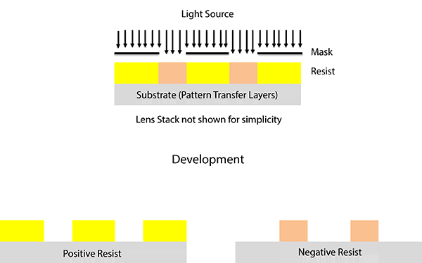
So how do we make lines for semiconductor manufacturing? Well, we use a process called lithography. Litho means light and graphy means write. If that makes you imagine burning ants with a magnifying glass you aren’t far off. In modern lithography, single wavelength light passes through a patterned mask and then through an absurd number of lenses in a lens stack before reaching the surface. The surface itself is covered with a material called a photoresist. Photoresists are designed to either become harder to rinse away or easier to rinse away when exposed to light.
We call the former positive resists because they create an image that’s the exact same as the mask, and the later negative resists because they invert the mask image (figure 2).
Now all of this is useful if you can’t transfer this pattern into something useful, which for most modern processors means metal wires in an insulator called dielectric. We’ll talk about etch and deposition a bit later, but for now just keep in mind that pattern transfer is the only reason we care about lithography.
Now we can make lines but we want to make them small. Think back to those squares on the paper (you didn’t skip the exercise did you?). Imagine drawing those squares with a sharpie or a fine point pen. Obviously a finer pen makes a finer line, and for lithography this means a finer beam of light (smaller wavelength). This is because light diffracts as it passes through holes of a similar size to its wavelength.
As the hole gets smaller the diffraction gets worse (figure 3).
This means that smaller holes in the mask actually result in larger (and blurrier) features in the resist. In order to write the smallest possible features, you want the smallest possible wavelength of light, but you also want the best possible lens.
$$ CD=k\frac{\lambda}{NA} $$
This brings us to the holy grail equation of Optical Lithography which says the smallest feature (we call this your Critical Dimension or CD) you can possibly print is equal to k (an efficiency factor) times the wavelength divided by the Numerical Aperture ( NA ) of the lens system. As a note if you instead care about pitch you just double this number.
So we talked about smaller wavelength helps (cuts down pesky diffraction), but what about NA? Well the common strategy to counteract the diffraction problem is to add a focusing lens stack below the mask. This allows for the light that is diffracted to be caught and redirect towards the sample. It also allows for the light to be focused and magnified to 4x or 5x the mask resolution. (eg a 5 inch square mask is commonly used which results in a 1 square inch size feature to be patterned). These lens systems are incredibly complex, large and expensive.
See the photo of the Zeiss lens stack as implemented in an ASML scanner for more.
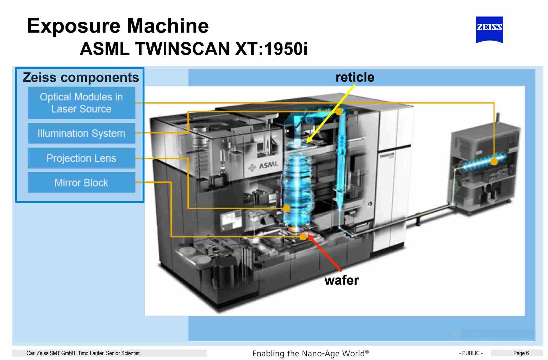
Way up at the top goes the mask (here called a reticle), and far below lies the wafer. The main limiting factor here is that it is very hard to make high NA lens stacks, they must be perfect, defect free, and must precisely magnify features across the reticle without distortion. The other thing is that lenses are symmetric. If a high NA lens captures more light on the inlet it should also spread more light on the outlet. The trick here is to immerse the outlet side of the lens in a high index of refraction fluid. This way because the light goes from a high NA lens to a high index of refraction fluid the light isn’t spread on the outlet at all. In immersion lithography the liquid is always water, as it’s available in very high purity and is used throughout the lithographic process.
Well but what about k? K describes and encompasses all that I will call ‘stupid optical tricks’. Now we talked about diffraction through a single hole in the mask, but remember all functional devices are made out of periodic arrays of lines.
Follow along on Figure 5 (based off a great figure by Shigeru23).
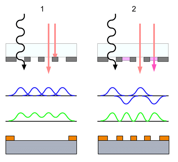
What happens when you have diffraction of nearby holes overlap (Black)? The answer is that the diffracted light builds up constructively to create a blurring of features (Green). At small enough sizes this prevents you from resolving the individual lines as shown at the bottom. That is to say your photo resist no longer sees them and it all goes away. To get around this we can use phase shifting masks which shift the light as it goes through every other hole in the mask. This causes adjacent holes to destructively interfere instead of constructively which produces nice sharp features (right side of the figure). Similarly, we can play with the angle that the light goes through the mask to further influence how the light constructively and destructively interferes. This is called off axis illumination and many improvements have come from simulating the best possible light pattern (combination of angles) to reliably print features on the sample.
Putting it all together: Back in the 70s we used 436 nm wavelength light, and 0.16 NA lenses with a k of 1 to produce ~2700 nm (2.7 micron or ~ 1/20th the width of your hair) features. Now a days we use an ArF excimer laser to make 193 nm wavelength light with fancy 1.33 NA immersion lenses and a k of around 0.3 which let’s us print 40 nm (130 carbon atoms or so) features. This means that the smallest pitch features possible with photolithography currently is about 80-84 nm. But aren’t people shipping processors on a 10 nm node? With 32 nm minimum pitch? How is that done?
Tune in next week and we’ll talk density multiplication. Or maybe deposition or etch.

Smart Guy & Technical Writer
PhD Candidate studying nanofabrication at University of Chicago