How To Write Small and Do Other Things Small Part 3: Etching
Published:
by:
Moshe Dolejsi
Last Updated:
Estimated reading time: ~12 minutes
So we’ve talked about lithography, and we’ve talked about EUV, as well as how we avoid using EUV, but why exactly do we do lithography?
| Fig.1 |
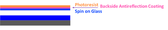 |
The purpose of lithography is patterning, and to realize that pattern you have to transfer it into your active material. Often this active material is several layers below where we have done our lithography (Fig1). So real quick, what are these extra layers and what are they doing keeping our precious pattern away from our good stuff?
- When light reflects off a surface, it can interfere with the light coming in. The solution is a backside antireflection coating.
- To prevent the patterned resist from toppling, its height can be at most twice the width of the smallest feature (imagine making a jello version of a skyscraper. Good luck). Best practice is to keep the thickness of the resist less than the pitch of the features patterned. Especially with Litho-Etch Litho-Etch strategies, or EUV where you directly pattern small features you might not have enough resist to serve as an etch barrier for pattern transfer. Thus the idea of a transfer stack (here showing spin on glass/spin on carbon stack).
How exactly do we go about transferring this pattern?
The simplest strategy is to take the thinnish photoresist (soft squishy organic) and transfer it with etching into a slightly thicker (35 nm ish) Spin on Glass (SOG, it’s Silicon Oxide ish) then you can take this slightly thicker pattern in SOG and transfer it into an even thicker (100 nm ish) Spin on Carbon (SOC, it’s charcoal/graphite esque).
| Fig.2 |
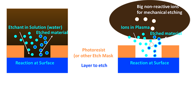 |
That’s well and good but how do we etch? We have two main options which are a wet etch or a dry etch (refer to figure above). As you can see they both look pretty similar. In the case of a wet etch, you have some etchant, often in water, and when you place your sample in it the etchant can’t react with your masking material (or perhaps it does but very slowly), but can react with the layer you want to etch. The key here is that the product of this reaction has to be water-soluble so that it can dissolve away. On the other hand we have a dry etch. In a dry etch we often use similar chemistry to wet etch, but instead of delivering the etchant in water, we instead inject gas into a chamber under vacuum (usually 1-5% atmospheric pressure) and ignite a plasma with a bunch of voltage. Ions from the plasma can be driven to the surface where they react, and here the key is the product has to be volatile (evaporate). If it is not we can add some unreactive gas (Helium, or Argon is common) to help a little bit physically scrub away the products.
| Wet Etch | Dry Etch |
| Low Capital | High Capital |
| High Chemical Use | Low chemical use |
| Chemical only | Physical or Chemical |
| Good control | Very precise control |
| Isotropic or Crystallographic | Anisotropic or Isotropic, (crystallographic more difficult) |
| High Etch Selectivity | Variable Etch Selectivity |
| Very Fast | Slow to Slower |
| 1 micron+ features | 15 nm+ feature sizes (smaller is just hard) |
| N/A | Combining with deposition in same tool allows for near infinite etch depth (Deep Silicon Etch) |
These two different options have very different properties summarized in the table above. Of course there is also a third option called Chemical Mechanical Planarization (CMP). Think rotary sander with a special chemical slurry that magically flattens any surface with incredible precision. Unfortunately it is not present at the academic level so I cannot comment on it, beyond that it is key for flattening each metal layer flush before beginning to pattern the next layer. Just remember it can only make things flat. That said let’s get into the comparisons.
| Wet Etch station (plastic tupperware) | Dry Etch (Plasmatherm ICP RIE) |
 |
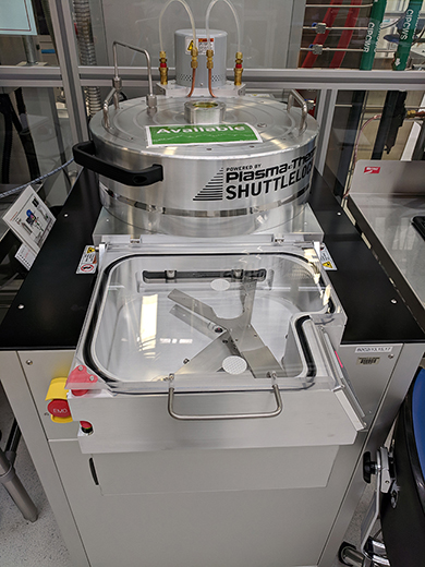 |
Cost: Wet etching is super cheap to set up. People set up baths with ferric chloride all the time in their garages to etch their own circuit boards. All you need is a cup or so of etch solution and a bunch of water to rinse with afterwards. On the other hand a decent Reactive Ion Etcher (RIE) w/ Inductively Coupled Plasma (ICP, more on that later) is going to cost you at least 100k not to mention the need to handle dangerous compressed gasses. What does that cost get you? The short answer is a whole lotta knobs to turn. One immediate advantage though is that plasma etchers use a whole lot less chemicals per etch then wet etching. When you are pumping out a few million wafers a month this represents a big savings for a relatively small capital investment.
| Fig.3 |
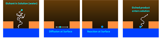 |
Wet etching: Let’s break down our simple picture from earlier into discrete steps to figure out how it all works. First whatever chemical were using to etch our surface has to find its way down to the surface. This diffusion can be very slow when holes are very narrow. Think about a game of pinball where the ball has to make it into a tiny slot, except it’s even worse because your etchant is going to be bouncing off water in your solution the entire way. The technical term for how far the etchant travels before it hits something is called, ‘Mean Free Path’ and the mean free path is pretty low for liquids because they are dense. Once the etchant hits the surface it wanders around for a bit until it finally reacts. Then the reacted product has to diffuse away from the surface in the same pinball manner.
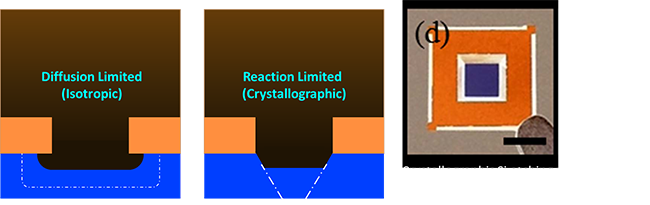
You’ll notice we haven’t talked about directionality, so how do we etch down? The answer is that as etchant reacts at the surface the local concentration of etchant drops, so you get a small concentration gradient which allows diffusion to occur. Depending on whether the diffusion is quicker than the reaction or vice versa you get one of two profiles. In the case where reaction is really quick but diffusion limits your etch you what is called an isotropic etch and as you can see, you have to etch left and right the same amount as you etch down. If your etching say mm width traces into a few microns of copper on a circuit board. The fact that you etch a few microns into those really wide traces just doesn’t matter. In fact as long as your feature is ~ 100x wider than it is tall you’re probably fine with this. In the other case where reaction limited you get something somewhat special. It turns out for many crystaline materials (including the Silicon we all know and love) that it’s atomic structure is a little bit different depending on how you look at it. For Silicon the [111] crystal plane is very tightly packed which makes it very hard for etching molecules to get in. As a result many wet etchants such as good ol drain cleaner (pottasium hydroxide) etch that plane very slow compared to the other planes. Another fun result of wet etching is because the etchant isn’t really forced to the surface you can get very high etch contrast. Etch contrast means you etch one material much faster than another which allows you to basically etch the fast material until you hit the slow material. These characteristics make wet etches incredibly useful for micro manipulators and micromechanical objects. As an example I’ve taken a figure from one of our groups papers1 where Jiaxing Ren (now at Lam Research 🙂 ) used KOH as a crystallographic Silicon etch with a Silicon Nitride etch stop layer. The KOH etches the [100] plane 400 times faster than the [111] plane and it etches silicon nitride about a thousand times slower than silicon. That made it easy for him to make a bunch of these thin (100nm or less) delicate & transparent membranes that we use to do all sorts of cool 3D imaging.
| Fig.4 |
 |
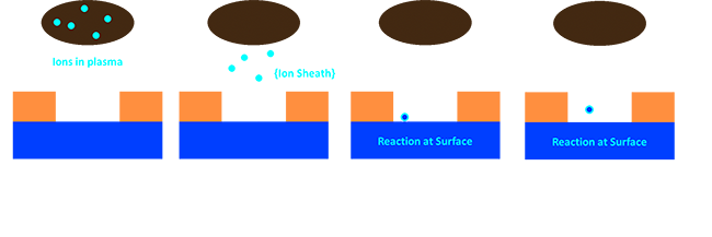
Dry Etching: We’re going to again start by breaking down the etch process. We start by loading our samples into the etcher. The etcher will pump down to very high vacuum (approximately eight orders of magnitudes less pressure than atmospheric) this is important to make sure the only gases in the plasma are those we select. Then the tool will flow in a controlled mixture of gases. In practice these are Oxygen (etches carbon to make CO2), fluorine containing (makes metal fluorides), chlorine containing (makes metal chlorides), or physical etchants like Helium and Argon (slam into surface meteor style). Which one you pick has a lot to do with the boiling point of the etch products formed, as well as the relative etch contrast of your surface/mask. Once the pressure is stabilized at the desired set point (usually 5 orders below atmospheric), the plasma is ignited. This is done by applying an AC bias from the sample holder across the chamber to ground. Too high a bias and you might form a conductive path and short the plasma, and too low a bias won’t make a plasma. That said modern tools make it very easy to find the right recipe. Modern tools also have an extra option to create an Inductively Coupled Plasma (ICP). These, ICP etchers can also create an additional AC bias across the plasma but not from your substrate. This is important because it lets you create more or less plasma without creating more acceleration of the plasma towards your sample. Speaking of acceleration towards the substrate, that whole ping pong effect that results in smearing out our wet etches just isn’t really a thing in dry etching. At very low pressures like those of dry etching, mean free paths become very very long (which can be its own problem). Once the ions hit the surface they either sputter material by slamming into it, or they react to form some etch product. This etch product then evaporates off the surface. If it isn’t very volatile we may increase the temperature of the surface to help out, or we may add more physical etching ions like Argon, or we may just increase the bias. The nice thing is that the etch products are neutral, and so we can drive ions to the surface with a bias, and it won’t trap our etch products.
| Fig.5 |
 |
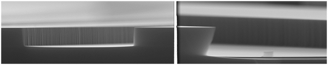
What does all this mean? It means we have a silly amount of knobs to really get whatever result we want. Because there are a low number of collisions and a high degree of directionality due to the driving voltage we tend to get etching more down than out. We call this anisotropic etching. Just as an example here are two Silicon etches that were done in the same tool at the Pritzker Nanofabrication Facility by one of our process engineers with the same gas chemistry but different ICP power. On the right, you can see that there is a bit of an undercut. This is because this etch used a far higher ICP power which resulted in a higher plasma density and thus more collisions. Most of the ions still went down of course, but some of them got knocked off course to the left or right causing the undercut.
| Fig.6 |
 |
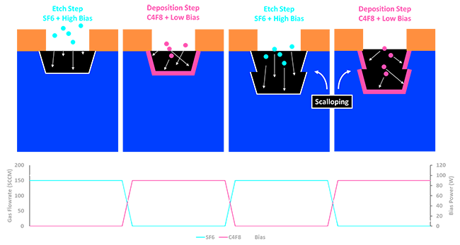
Deep Silicon Etching : Even more dramatically is the case of Deep Silicon Etching (DSE). DSE is used to bore Through Silicon Vias (TSV) all the way through hundreds of microns of wafer. Even for a dry etch it would be impossible to do this with a single set of settings. Even the most anisotropic dry etch still slightly etches left and right as it goes down. So how do we etch TSV or make 90+ stack 3D nand? The answer is the Bosch Process which I’ve illustrated in the following figure. We basically etch the silicon just a little bit, using SF6 as an etch gas with a strong bias to really etch down as straight as possible. At this time, we’re also getting a bit of etching to the left and right. Then without cutting the plasma we feed in C4F8 instead of SF6. It turns out that Fluorine plasmas that contain a lot of carbon, like that of C4F8, tend to deposit a lot of fluoropolymer everywhere. So by using C4F8 and dropping the bias we can basically put a fresh protective layer over all the exposed surfaces. Then we swap back to SF6 and start etching again. At this point we again start slowly etching left and right, but because the sides are protected we don’t expand the hole in that direction and instead we just start slowly etching the fluoropolymer. Meanwhile the fluoropolymer at the bottom of the hole is quickly punched through by the high bias. This creates a very characteristic scalloped sidewall that is associated with all DSE processes. Once we get to the point that we’ve worn through that protection on the sides of the hole we swap back to deposition. These cycles can be done hundreds of times to create TSV.
| Deep Silicon Etch Scheme |
 |
Hopefully this gives you a bit of flavor as to why dry etching with plasma is so important. Of course, wet etching still has its place, but when you’re talking small features it’s hard to argue with the amount of control you get with plasma. The only tighter process is something new on the scene called Atomic Layer Etching, but that is essentially isotropic only and we will cover that with Atomic Layer Deposition (ALD), which will hopefully be part of my next article on Deposition in general.

Smart Guy & Technical Writer
PhD Candidate studying nanofabrication at University of Chicago