What's the big deal with EUV (Extreme UltraViolet)?
Published:
by:
Moshe Dolejsi
Estimated reading time: ~11 minutes
When last we spoke we talked a bit about how we use photolithography to write very small features. We also talked quite a bit about the governing equation for lithography.
$$ CD=k\frac{\lambda}{NA} $$
We talked about how tricks like off axis illumination and phase shifting masks can be used to lower k, and we talked about how immersion lithography allows us to maximize our Numerical Aperture (NA). However, we talked very little about λ or wavelength, aside from the fact that lower is better. So why can’t we just use much smaller wavelengths?
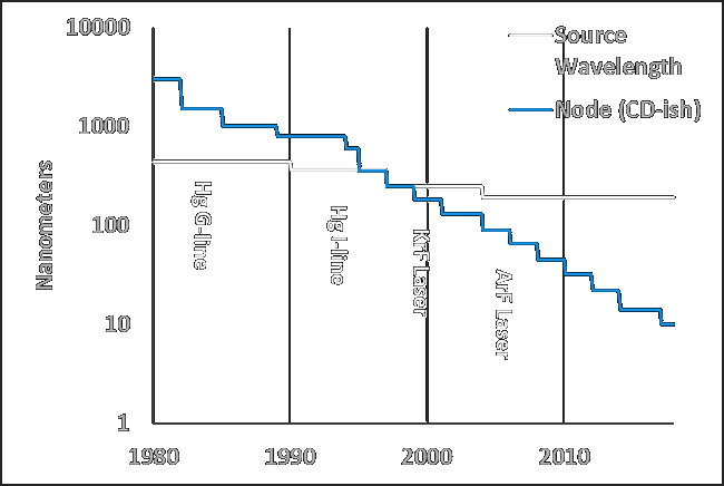
Turns out that over the years we have shrunk the wavelength of light used for photolithography but at nowhere near the same rate as we have shrunk the critical dimension (CD). Here I’ve plotted the ‘Node’ (~ CD) as well as the wavelength of light used for that node. As you can see, we used to have CD > Wavelength which is lithographically easy. We don’t need to do any tricks to lower k below 1 and we don’t need to do any tricks to raise the numerical aperture (NA) above 1. Then in the 1990’s we got to the point where now we need feature sizes a little bit smaller than the wavelength. Now we need to start being careful. Then finally in 2004, we get to the point where the sizes are now less than half the wavelength of light being used, and things get really hard. We need high-NA lithographic tools (immersion), and we need low k processes (off axis illumination, phase shifting masks) and that barely works. Today with a 193 ArF laser and all of these tricks, the limit is a pitch of ~82 nanometers so feature sizes of about 40 nanometers. We’ll talk next time about how we use density multiplication ($ $ $ $) to cheat our way smaller but for now. Wouldn’t it be nice if we could just shrink the wavelength more?
Fun question: Why have we evolved to see the visible spectrum?
Answer: Because light at lower wavelengths is absorbed by everything so it isn’t useful to see.
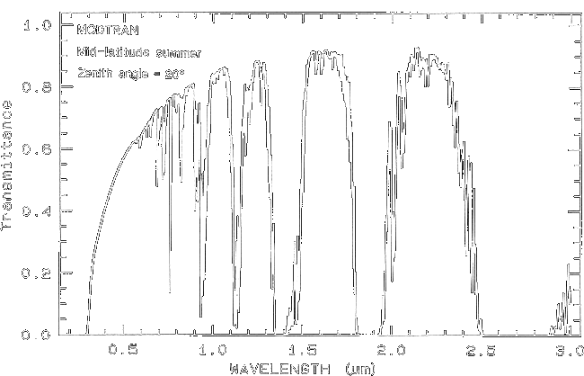
Berk et al 1989.
Note how transmittance of the atmosphere drops like a rock below 200 nm?
This means that going below 193 nm immersion, 193i, (ArF laser source) requires not just a completely new source, but also a completely new optics train, not to mention a completely new resist material, and it all needs to be done in vacuum with the light passing through nothing. It’s not any surprise then that 157 nm (F2 laser source) was investigated and dropped like a rock in 2004. If we want to go lower, we need to go low enough that we offset the pain with enough gain to make it worth it. And that brings us to Extreme Ultra Violet or EUV which is 13.5 nm wavelength. Luckily, we’ve been working on EUV for decades which gives us decades of humorous graphics to go on. You think 10 nm’s delay is bad? How about EUV.
So just what has delayed tools from 2004 to today, where there is still no HVM manufacturing underway with EUV? First the optics train.
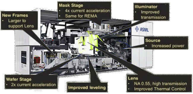
Before we could center all the lens about the light, but the first rule of EUV is everything absorbs EUV, and that means mirrors must be used for focusing. Compare the ASML high-NA EUV tool pictured above to the 193i stepper in my previous article to see the difference. The newest tools that people are looking at today in particular have 10 mirrors. These mirrors are made of alternating stacks of Molybdenum and Silicon each layer a precise thickness close to 3.4 nanometers (1/4th the wavelength) to maximize possible reflections. This arrangement is called a Bragg stack or Bragg reflector, as it is based on Bragg’s law to maximize reflection at a given wavelength. Why close to 3.4? Because some of the mirrors are non-spherical and some of the light hits the mirrors at different angles across the mirror. This means the thickness of the layers need to vary in a precise manner across each mirror. That’s not even the hard part about the mirrors. The hard part is that these perfectly alternating stacks, might reflect as much EUV as possible, but the best mirrors are still only about 70% reflective. That means that in total your ten mirrors will absorb 97% of all the light you pump into your tool, which means a lot of heat, which means a lot of expansion, which means those perfect thicknesses are tough to maintain.
Sure, that sounds difficult but what about the mask? Well for 193 immersion the mask is quartz and as the light passes through the mask it hits the chromium and is absorbed. Of course, for EUV the light would just be absorbed by the quartz (EUV rule 1), so instead the mask is also a mirror. Because the mask is a mirror that means it must be placed off angle from the wafer so that light can come in from the previous mirror and hit the wafer. This means two things. First, the light hits the mask at different angles across the mask, which means the mask must be corrected for shadowing effects. Second, the mask, like all those other mirrors, absorbs about 30% of the light that hits it (+100% wherever there is a patterned feature). This means the mask heats up, which makes the mask expand several nanometers, which wrecks your writing. Not only that but masks tend to be very expensive to make, a full mask set can be hundreds of thousands of dollars. Traditionally masks are protected with a thin layer called a pellicle. If dust lands on the mask rather than getting a whole new mask, the pellicle can be removed with the dust and a fresh pellicle placed on, but of course EUV rule 1 prevents a pellicle from being used (though some investigation is going into carbon nanotube-based pellicles that might absorb little enough so as to be useful). As if that wasn’t enough because of the complicated light path, not only does the mask need to be corrected for different light exposure as the tool scans across the mask, but there is also a large tool to tool variation as shown by Mentor Graphics at Lithovision 2017.

Notice how the variation across slits for a single EUV tool is greater than the variation across three different 193 immersion (DUV) tools. As if that wasn’t enough, don’t forget that because the mask isn’t center with the wafer and is instead exposed at an angle that there are different effects if we ever need to go to off axis illumination to get a low k. Speaking of which. Where exactly has EUV got us so far? Well let’s go back to our governing equation and pretend we want to make the tightest pitch on Intel’s 10 nm node (32 nm). We can plug in 16 nm for CD (half pitch), and 13.5 nm for wavelength, and the state-of-the-art numerical aperture for the currently available NXE3400 EUV tool by ASML is… 0.3, which means the k required is 0.36. That means Intel would need off axis illumination to print their tightest layer. Except every different set of features you could imagine has a widely different optimum illumination, which changes across the slit, and changes from tool to tool. Even the new NXE3500 with its higher NA of 0.55 doesn’t quite cut it. (I could talk about the tricks needed for high NA, but this is long enough)
$$ CD=k\frac{\lambda}{NA}\;or\;16nm=k\times\frac{13.5}{0.3}\;so\;k\;required=0.36 $$

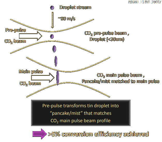
Now let’s talk source, and then in particular source power, and its closely related demon of necessary photoresist dose. So, what is our source for 13.5 nm light? We mentioned before that we use ArF excimer lasers for 193, so if you guessed a laser come up and collect your prize. For 13.5 nm we use a laser produced plasma (LPP) from tin droplets. Molten tin is filtered, and then dropped into a chamber. As it drops it is hit by a shaping pulse which flattens the droplet to match the shape of the main pulse. The main pulse (~30 KW) then hits the tin ‘pancake’ and forms a plasma that emits at best 6% of that power as 13.5 nm light, which is then dropped far further by mirror absorption as we talked about earlier. What happens to the rest of the tin droplet? Well it somewhat sputters all over the place, some of it is collected and some of it is removed via hydrogen cleaning. EUV tools have about 70%-80% uptime mainly due to how maintenance intensive the source is, and eventually it needs to be replaced due to tin build up.
So, what about the source power? Essentially for EUV scanners to be worth it, the benchmark is to produce 125 wafers per hour which is approximately half as many as 193i. If you increase the source power you decrease the wafer writing time, on the other hand increasing the dose (Energy) will increase the wafer writing time. There is overhead for moving the wafer around and loading and unloading the wafer. Loading and unloading in particular is slow that state of the art tools support two wafers at once so that when one wafer is exposed it can be removed and replaced while the other wafer is exposed (ASML calls this twinscan). So where are we at today? Thankfully we don’t have to do the math because ASML has done it for us for both the current best and their new high-NA tool (which no one will have until 2021). You’ll notice quite coincidentally how their current tool can produce exactly 150 wafer per hour with a source power of 500W (double what has been demonstrated even by ASML) at a dose of 30 mJ/cm^2. In comparison their new tool (again it won’t even be arriving at fabs for evaluation until 2021) produces exactly 150 wafers per hour at a dose of 60 mJ/cm^2 using the same source power.
What if we just use their current tool, with a source power of 250, and a dose of 30? We get 80 wafers per hour. Oof. Let’s just look at the current tool with 0.33NA and now consider feature size, again ASML has done the math for us though you’ll notice they did it with a higher source power then is available (again). Exposing the tightest features on Intel’s 10 nm node already requires two separate EUV exposures, which means even with a source power 100W higher than what is currently available you can’t even expose 80 wafers per hour. Double oof.
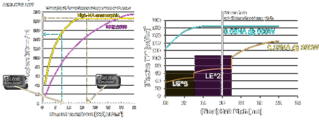
One last thing. Why are those lines curved? Why does the throughput drop as you drop feature size? It’s because EUV is very high energy. To get the same dose at 13.5 nm as you did at 193 nm you use an order of magnitude less photons. That means that the natural variation in photons so called photon shot noise is far more important across a constant dose/area. So, we do some math and find out that at a 10 mJ/cm^2 dose for 193i we get 97 photons per nanometer squared, which means shot noise contributes +/- 10%. At the same dose, with EUV, shot noise is now +/- 40%! To bring it back down we have to increase the dose. And as we shrink features the necessary dose just rises and rises.
$$ Photon\;Shot\;noise\cong\frac{1}{\sqrt{Photons}}=\frac{1}{\sqrt{97}}\sim10\%(193i)\;or\;\frac{1}{\sqrt{6.7}}\sim40\%(EUV) $$
This brings us to the problem with these plots. If we compare them to each other it appears as though they are using a dose of about 20 mJ/cm^2 at a half pitch of 22 nm (350⁄20 = 17.5 which per the left chart is ~ 150 wph matches up nicely with the right chart). As you go smaller at 20 nm half pitch the wph drops a bit to account for the shot noise and is now 135, per the chart on the left that means a modest increase of dose to about 23 mJ/cm^2. Here is the problem: Per their own brief on the NXE3400 (the brand new 0.33 NA aperture tool they are just now selling with a source power of 250) they use an exposure dose of 76+18 mJ/cm^2 to resolve features from 24 nm to 18 nm. (with by the way variance still too high to use for lithography). This means the WPH on the figure on the right is really 3 times too high! Of course, these three figures are never presented side by side by ASML.
TLDR: There has been a lot of work on EUV by many people and a lot of challenges have been overcome, but right now even trying to make 20 nm CD (40 nm pitch) features with the state of the art NXE3400b with a source power of 250W requires a dose of roughly 80 mJ/cm^2 which means you can only make 40 wafers per hour. It’s just not cost effective, and no one knows when it will be. In the meantime, we need to use density multiplication to extend 193 immersion. Stay tuned for an article on that.

Smart Guy & Technical Writer
PhD Candidate studying nanofabrication at University of Chicago